USB2.0-Camera-Shield-Rev.E
Introduction
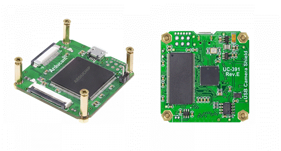
This chapter describes the operation of the ArduCAM USB2 camera shield. The latest device driver, SDK library, and examples can be downloaded from here The highlight of the new USB2.0 camera shield Rev.E is that it supports MIPI interface sensors without any MIPI adapter board. It has onboard 16MByte hardware frame buffer, and overcome the bandwidth and dropping frames issue when using the software frame buffer scheme. In addition, with the onboard frame buffer, it supports synchronized multiple cameras taking images exactly at the same time. Now it well supports both PC and an embedded system like Raspberry Pi, and also can provide customized support for Odroid, Beaglebone Black, Nvidia Jetson TK/TX boards.
Hardware
Hardware Installation
Figure 1. Interface Diagram:
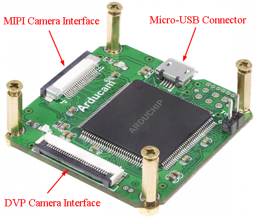
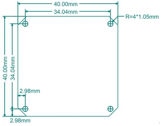
Figure2. Arducam USB2 Camera Shield Mechanical Dimension:
There are two different camera interface provided on the USB camera shield, but only one camera interface can be used at a time.
MIPI Camera Interface
The MIPI camera interface is used for the 22 pin MIPI camera breakout board. Visit the Featured Camera Modules Supported chapter to see the full list.
| Pin No. | PIN NAME | TYPE | DESCRIPTION |
| 1 | GND | Ground | Power ground |
| 2 | D0_N | Input | MIPI DATA0 N |
| 3 | D0_P | Input | MIPI DATA0 P |
| 4 | GND | Ground | Power ground |
| 5 | D1_N | Input | MIPI DATA1 N |
| 6 | D1_P | Input | MIPI DATA1 P |
| 7 | GND | Ground | Power ground |
| 8 | C_N | Input | MIPI CLOCK N |
| 9 | C_P | Input | MIPI CLOCK P |
| 10 | GND | Ground | Power ground |
| 11 | D2_N | Input | MIPI DATA2 N |
| 12 | D2_P | Input | MIPI DATA2 P |
| 13 | GND | Ground | Power ground |
| 14 | D3_N | Input | MIPI DATA3 N |
| 15 | D3_P | Input | MIPI DATA3 P |
| 16 | GND | Ground | Power ground |
| 17 | PWEN | Output | MIPI Power En(active HIGH) |
| 18 | VCC | POWER | 3.3v Power supply |
| 19 | GND | Ground | Power ground |
| 20 | SCL | Input | Two-Wire Serial Interface Clock |
| 21 | SDA | Bi-directional | Two-Wire Serial Interface Data I/O |
| 22 | VCC | POWER | 3.3v Power supply |
The DVP camera interface is used for the camera breakout board with 30pin ribbon cable. Visit the Featured Camera Modules Supported chapter to see the full list.
| Pin No. | PIN NAME | TYPE | DESCRIPTION |
| 1 | GND | Ground | Power ground |
| 2 | NC | - | - |
| 3 | Trigger | Output | Exposure synchronization input |
| 4 | VSYNC | Input | Active High: Frame Valid; indicates active frame |
| 5 | HREF | Input | Active High: Line/Data Valid; indicates active pixels |
| 6 | DOUT11 | Input | Pixel Data Output 11 (MSB) |
| 7 | DOUT10 | Input | Pixel Data Output 10 |
| 8 | DOUT9 | Input | Pixel Data Output 9 |
| 9 | DOUT8 | Input | Pixel Data Output 8 |
| 10 | DOUT7 | Input | Pixel Data Output 7 |
| 11 | DOUT6 | Input | Pixel Data Output 6 |
| 12 | DOUT5 | Input | Pixel Data Output 5 |
| 13 | GND | Ground | Power ground |
| 14 | DOUT4 | Input | Pixel Data Output 4 |
| 15 | DOUT3 | Input | Pixel Data Output 3 |
| 16 | DOUT2 | Input | Pixel Data Output 2 |
| 17 | DOUT1 | Input | Pixel Data Output 1 |
| 18 | DOUT0 | Input | Pixel Data Output 0(LSB) |
| 19 | NC | - | - |
| 20 | PCLK | Input | Pixel Clock output from sensor |
| 21 | SCL | Input | Two-Wire Serial Interface Clock |
| 22 | SDA | Bi-directional | Two-Wire Serial Interface Data I/O |
| 23 | RST_N | Output | Sensor reset signal, active low |
| 24 | GND | Ground | Power ground |
| 25 | GND | Ground | Power ground |
| 26 | STANDBY | Output | Standby-mode enable pin (active HIGH) |
| 27~30 | VCC | POWER | 3.3v Power supply |
Driver Installation
The Arducam USB camera shield is not a standard USB Video Class device. Instead, it uses a private driver for our proprietary SDK and API that helps you access all the sensor features from the register level. Check the Windows Driver Installation chapter to learn about how to install the driver.
Demo Code
Arducam provides a comprehensive SDK library and API for C++ and Python. Besides, we offer a GUI Windows program that helps you easily understand the operation of the ArduCAM USB camera and SDK library. Check the Software SDK and API chapter to learn more about how to run the demo.
Register Table
| register address | register type | UC-391 Rev.E (USB 2.0) |
| 0x00 | read-only | bit[7:0]:CPLD version number UC-391 Rev.E:0x25 |
| 0x01 | read-write | bit[7]:DVP Camera 8/16bit 0: 8bit;1: 16bit bit[5]:DVP Camera pclk polarity 0:normal;1:inverse bit[4]:ircut 0:on;1:off bit[3]:DVP Camera standby 0:normal;1:standby bit[2]:DVP Camera rst_n 0:rst;1:normal bit[1]:MIPI Camera standby 0:normal;1:standby bit[0]:MIPI Camera rst_n 0:rst;1:normal |
| 0x02 | read-write | bit[8]: Select the external trigger connected to CPLD by DVP camera as input or output of CPLD 0:CPLD input;1:CPLD output bit[4]: Choose whether the internal simulative data a counter or a color bar 0:color bar;1:counter bit[2]:simulative data/camera data 0:camera data;1:simulative data bit[0]:DVP Camera vsyn polarity 0:normal;1:inverse |
| 0x03 | read-write | bit[7]:cpld reset 0:normal;1:reset Set it to 1 and then set it back to 0 bit[6]:Pause Camera Data Input 0:normal;1:pause bit[5]:Single shot (Not valid until bit [6] is 1) 0:wait;1:Start a single shot Set it to 1 and then set it back to 0 |
| 0x04 | read-write | bit[7:0]:Frame skipping function Because the number of input frames may be faster than the bandwidth of USB 2.0, the number of uploaded frames can be reduced by frame hopping M=bit[7:4] N=bit[3:0] Normally, for each N frame, take M frames 0x00,No frame skipping 0x01,Skip 1 frame.That's1/2(To be compatible with Rev.C.) 0x11,No frame skipping 0x12,1/2 0x13,1/3 …… 0x1F,1/15 |
| 0x05 | read-only | bit[7:0]: CPLD version year For example decimal 19, the upper machine-readable register value will be added 2000, indicating 2019 |
| 0x06 | read-only | bit[7:0]: CPLD version month For example: decimal 08, for August |
| 0x07 | read-only | bit[7:0]: CPLD version date For example decimal 03, for 3 |
| 0x08 | read-write | bit[7]:Is data uploaded to USB 0:normal;1:Stop uploading bit[0]: Upper computer clears finish ID of single-shot mode 0:Not clear up;1:clear up Set it to 1 and then set it back to 0 |
| 0x09 | read-only | bit[0]: finish ID of single shot mode 0:unfinished;1:finished |
| 0x0A | read-write | bit[1:0]:Data bit Selection of DVP Camera DVP Camera,The input data is 12 bits 【8-bit mode】 0:dvp_data[11:4] 1:dvp_data[9:2] 2:dvp_data[7:0] 【16-bit mode】 0:{4'd0, dvp_data[11:0]} 1:{6'd0, dvp_data[9:0]} |
| 0x0B | ||
| 0x0C | read-write | bit[7]: Camera Selection 0: DVP Camera;1:MIPI Camera bit[4]:MIPI RAW format 0:raw8;1:raw10 bit[1:0]:MIPI channel 0:1Lane;1:2Lane;2:4Lane |
| 0x0D | read-write | MIPI, Image resolution, column, High 8 bits |
| 0x0E | read-write | MIPI, Image resolution, column, Low 8 bits |
| 0x0F | read-write | MIPI, Image resolution, row, High 8 bits |
| 0x10 | read-write | MIPI, Image resolution, row, Low 8 bits |
| 0x11 | read-write | bit[5:4]: ECC check mode 3:{DI, WC_I, WC_H} 2:{DI, WC_H, WC_I} 1:{WC_I, WC_H, DI} 0:{WC_H, WC_I, DI} bit[2]: WC Check of MIPI HREF 0:No check;1:check bit[1]: data_type check (Is it raw8 or raw10?) 0:No check;1:check bit[0],MIPI ECC check 0:No check;1:check |
| 0x12 | read-write | bit[7],Two Extended IOs as PWM or GPIO 0: GPIO;1: PWM bit[0]: GPIO Direction 0: CPLD input;1: CPLD output |
| 0x13 | read-only | bit[1:0]: GPIO read-in values bit[1]:GPIO[1] read value bit[0]:GPIO[0] read value |
| 0x14 | read-write | bit[1:0]: GPIO write-out values bit[1]:GPIO[1] write value bit[0]:GPIO[0] write value for example: If 0x12 writes 0x01, the two extended IO is GPIO,the GPIO[1] and GPIO[0] are both output then 0x14 writes 0x01, then GPIO[1] is low level, and GPIO[0] is high level |
| 0x15 | read-write | bit[5:4]: Selection of pwm_0 Cycle Counting Clock 3:320us 2:160us 1:80us 0:40us bit[1:0]: Clock selection for pwm_0 high-level counting 3:40us 2:20us 1:10us 0:5us |
| 0x16 | read-write | bit[7:0]: Number of High Level Width Clocks in pwm_0 |
| 0x17 | read-write | bit[7:0]: Number of pwm_0 Periodic Width Clocks |
| 0x18 | read-write | bit[5:4]: Selection of pwm_1 Cycle Counting Clock 3:320us 2:160us 1:80us 0:40us bit[1:0]: Clock selection for pwm_1 high-level counting 3:40us 2:20us 1:10us 0:5us |
| 0x19 | read-write | bit[7:0]: Number of Clocks with High Level Width in pwm_1 |
| 0x1A | read-write | bit[7:0]: Number of pwm_1 Periodic Width Clocks |
| 0x1B | read-write | |
| 0x1C | read-write | |
| 0x1D | read-write | |
| 0x1E | read-only | Read MIPI parsed information bit[7:0]: MIPI DATA ID |
| 0x1F | read-only | Read MIPI parsed information bit[4:0]: MIPI,Image resolution,column,High 5 bits |
| 0x20 | read-only | Read MIPI parsed information bit[7:0]: MIPI,Image resolution,column,Low 7 bits |
| 0x21 | read-only | Read MIPI parsed information bit[4:0]: MIPI,Image resolution,row,High 5 bits |
| 0x22 | read-only | Read MIPI parsed information bit[7:0]: MIPI,Image resolution,row,Low 7 bits |