Arducam Chip
1. Introduction
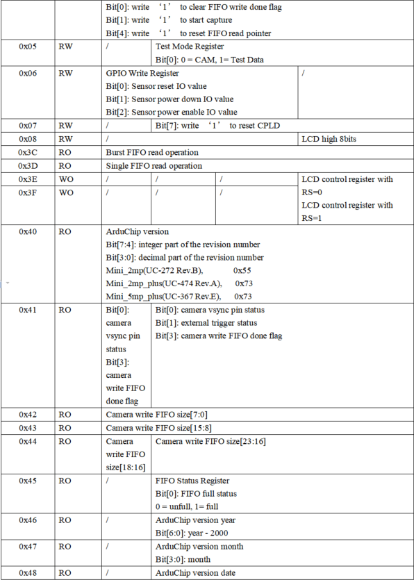
The ArduChip is ArduCAM proprietary camera controller technology which hides the complex camera, LCD screen, memory and user interface hardware timing into a chip level and provides a set of control registers and user friendly SPI interface.
2. SPI Interface Timing
The ArduCAM SPI slave interface is fixed SPI mode 0 with POL = 0 and PHA = 0. The maximum speed of SCLK is designed for 8MHz, care should taken do not over clock the maximum 8MHz. The SPI protocol is designed with a command phase with variable data phase. The chip select signal should always keep asserted during the SPI read or write bus cycle. The first bit[7] of the command phase is read/write byte, ‘0’ is for read and ‘1’ is for write, and the bit[6:0] is the address to be read or write in the data phase.
2.1 SPI Bus Write Timing
The SPI bus write timing composed of a command phase and a data phase during the assertion of the chip select signal CSn. The first 8 bits is command byte which is decoded as a register address, and the second 8 bits is data byte to be written to the ArduChip internal registers.
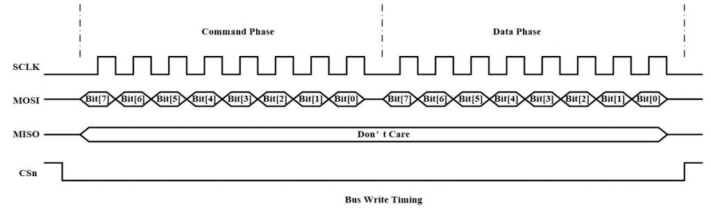
Figure 1 SPI Bus Write Timing
2.2 SPI Bus Single Read Timing
The SPI bus single read timing is for read operation of ArduChip internal registers and single FIFO read function. It is composed of a command phase and a data phase during the assertion of chip select signal CSn. The first 8 bits is command byte which is decoded as a register address, the second 8 bits is dummy byte written to the SPI bus MOSI signal, and the content read back from register is appeared on the SPI bus MISO signal.
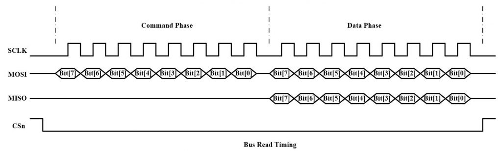
Figure 2 SPI Bus Single Read Timing
2.3 SPI Bus Burst Read Timing
The SPI bus burst read timing is only apply for burst FIFO read operation. It is composed of a burst read command phase and multiple data phases in order to get double throughput compared to the single FIFO read operation. (Note: Older Arducam spi cameras, the first byte read from the FIFO is a dummy byte, and the following bytes are valid bytes. )
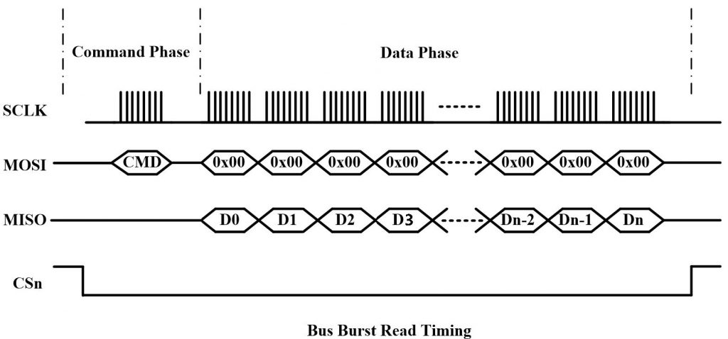
Figure 3 SPI Bus Burst Read Timing
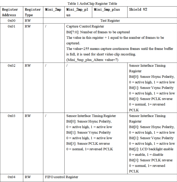
3. Registers Table
Sensor and FIFO timing is controlled by a set of registers which is implemented in the ArduChip. User can send capture commands and read image data with a simple SPI slave interface. The detail description of registers’ bits can be in this section.
As mentioned earlier the first bit[7] of the command phase is read/write byte, ‘0’ is for read and ‘1’ is for write, and the bit[6:0] is the address to be read or write in the data phase. So user has to combine the 8 bits address according to the read or write commands they want to issue.
Different ArcuCAM platform uses different ArduChip and has different functionalities. Here is a list of possible hardware platforms:
| Hardware Platform | Functions | |||||
|---|---|---|---|---|---|---|
| Single Capture/ Read | Burst Read | Multiple Capture | Rewind | Low Power Mode | Short Video Capture | |
| ArduCAM Shield Rev.C | √ | |||||
| ArduCAM Shield Rev.C+ | √ | √ | √ | √ | ||
| ArduCAM-Mini-2MP | √ | √ | √ | √ | ||
| ArduCAM-Mini-5MP | √ | √ | √ | √ | √ | |
| ArduCAM-Mini-5MP (Bit-Roation-Fixed) | √ | √ | √ | √ | √ | |
| ArduCAM Shield V2 | √ | √ | √ | √ | √ | |
| ArduCAM-Mini-5MP-Plus (OV5642) | √ | √ | √ | √ | √ | √ |
| ArduCAM-Mini-5MP-Plus (OV5640) | √ | √ | √ | √ | √ | √ |
It is a basic capture function of the ArduChip. The capture command code is 0x84, and write ‘1’ to bit[1] to start a capture sequence. And then polling bit[3] which is the capture done flag by sending command code 0x41. After capture is done, user have to clear the capture done flag by sending command code 0x41 and write ‘1’ into bit[0] before next capture command.
By sending the command code 0x81 and with writing the number of images to be capture into bit[2:0], before starting the capture command as the single capture sequence does. Please note that user should trade off between the resolution and number of images to be captured and do not make the frame buffer overflow.
Use the same command as the Multiple Capture Mode. When the value bit[2:0] equals to 7, the ArduCAM will continuously capture the images until the entire frame buffer is full. User can save the captured MJPEG to AVI files to create short movie clips.
It is basic memory read function which start a single read operation and read a single byte each time. By sending command code 0x3D to start a single read operation, a single byte is read out from the frame buffer.
It is advance capture function which can read multiple bytes out of the frame buffer by just sending a single command code 0x3C.
Please note that for these hardware platforms (ArduCAM Shield Rev.C+, ArduCAM-Mini-2MP, ArduCAM-Mini-5MP) the first read byte should be ignored in the first read transaction, because it is a dummy byte. In the following read transaction, the first byte read is the last read byte in the last read transaction, it is very important. And do not use other SPI command between burst read transaction. Detail timing can be found from Figure 5.
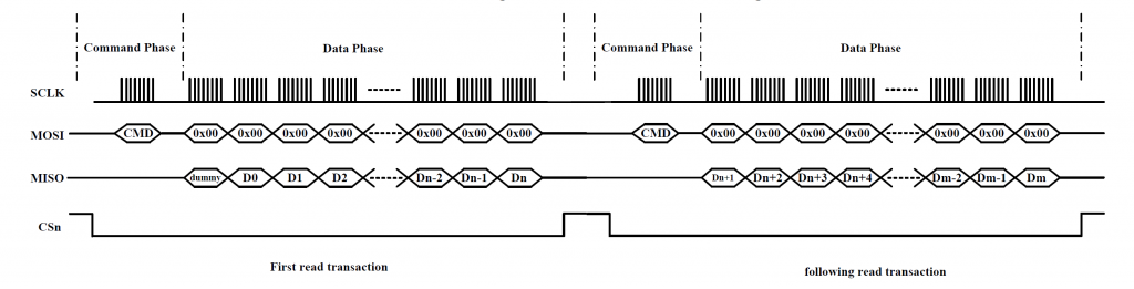
Figure 5 Burst read timing diagram 1
For hardware platforms (ArduCAM-Shield-V2, ArduCAM-Mini-5MP-Plus), you don't need to worry about the first byte. Detail timing can be found from Figure 6.
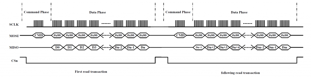
Figure 6 Burst read timing diagram 2
Rewind read is useful for some application that need access the same pixel data multiple times. By sending the command code 0x84 and write ‘1’ to bit[5] in the data phase, it will reset the memory read pointer to ZERO. Then user can read the image data from the start of the memory.
For some battery powered device power consumption is very important. There are two levels to achieve low power mode, user have to combine these modes according to their own power strategy.
It is achieved by controlling the power enable pin of the onboard LDOs. The power enable pin is controlled by the GPIO[2] of ArduChip. By sending the command code 0x86 and write ‘1’ to bit[2] to enable the LDOs, or write ‘0’ to bit[2] to disable the LDOs to save power. Note that power down the sensor circuit, the camera settings are lost. User should reinitialize the sensor when power up the sensor circuit again.
It is achieved by controlling the power enable pin of the onboard LDOs. The power enable pin is controlled by the GPIO[1] of ArduChip. By sending the command code 0x86 and write ‘1’ to bit[1] to set the sensor into standby mode, or write ‘0’ to bit[1] to set the sensor out of standby mode. Note that the sensor settings are not lost when in standby mode, and reinitialize is not needed.
Register Table
Sensor and FIFO timing is controlled with a set of registers which is implemented in the ArduChip. User can send capture commands and read image data with a simple SPI slave interface. The detail description of registers’ bits can be found in the software section in this document. Not all the registers are implemented in a given hardware platform, please check the hardware develop guide for detail register description for certain hardware you've got. As mentioned earlier the first bit[7] of the command phase is read/write byte, ‘0’ is for read and ‘1’ is for write, and the bit[6:0] is the address to be read or write in the data phase. So user has to combine the 8 bits address according to the read or write commands they want to issue.